Difference between revisions of "Geneve wait state generation"
Stephen Shaw (talk | contribs) (→Architecture: replace missing page link with expansion of abbreviation) |
|||
| (3 intermediate revisions by one other user not shown) | |||
| Line 1: | Line 1: | ||
In this section we shall discuss the wait state generation on the Geneve board. Wait states are required to slow down accesses, in particular, if the device being accessed cannot catch up with the speed of the CPU. | |||
Although scematics are available for the Geneve, the creation of wait states is hidden in two custom chips on the board - a registered PAL and the Gate array, both of which lack documentation. | |||
== Architecture == | == Architecture == | ||
| Line 5: | Line 9: | ||
[[File:Waitstates_arch.png | 500px | left ]] | [[File:Waitstates_arch.png | 500px | left ]] | ||
The CPU, the TMS 9995, contains an own set of memory locations at addresses >F000 to >F0FB and the remaining 4 bytes at the end of the address space, that is, >FFFC to >FFFF (which are the | The CPU, the TMS 9995, contains an own set of memory locations at addresses >F000 to >F0FB and the remaining 4 bytes at the end of the address space, that is, >FFFC to >FFFF (which are the NMI (None Maskable Interrupt) [[branch vector]]). The internal memory locations are directly connected to the 16 bit data bus, so we should say these are 128 words of 16 bit each. | ||
All other memory locations are outside of the CPU, and the 16 bit data transfers are converted to a sequence of two 8 bit data transfers. This is quite similar to the mechanism used in the TI-99/4A, with the exception that the TI send the odd address byte first, then the even address, and the TMS 9995 starts with the even address, followed by the odd address. | All other memory locations are outside of the CPU, and the 16 bit data transfers are converted to a sequence of two 8 bit data transfers. This is quite similar to the mechanism used in the TI-99/4A, with the exception that the TI send the odd address byte first, then the even address, and the TMS 9995 starts with the even address, followed by the odd address. | ||
Wait states can only be created outside of the CPU; there is no way of creating wait states within the CPU (possibly also no need). There is a special PIN called READY which is used for wait state creation. | Wait states can only be created outside of the CPU; there is no way of creating wait states within the CPU (possibly also no need). There is a special PIN called READY which is used for wait state creation. | ||
Instead, we have an external wait state generation. The gate array circuit is used to create wait states in certain situations. When a wait state shall appear, the READY line of the CPU must be pulled down (cleared). | Instead, we have an external wait state generation. The gate array circuit is used to create wait states in certain situations. When a wait state shall appear, the READY line of the CPU must be pulled down (cleared). | ||
| Line 81: | Line 84: | ||
which makes '''4 cycles''' or 1.332 µs execution time. | which makes '''4 cycles''' or 1.332 µs execution time. | ||
For a better overview we can use the following style: | |||
{| class="waitstate" | |||
|- | |||
! 1 !! 2 !! 3 !! 4 | |||
|- | |||
| MOV R1,@ | |||
| < R1 | |||
| F080 | |||
| > *F080 | |||
|} | |||
If the workspace is located in '''DRAM''' instead, we get more cycles: | If the workspace is located in '''DRAM''' instead, we get more cycles: | ||
| Line 89: | Line 104: | ||
* read the target argument (F080): 1 cycle | * read the target argument (F080): 1 cycle | ||
* write the contents to the target address: 1 cycle | * write the contents to the target address: 1 cycle | ||
{| class="waitstate" | |||
|- | |||
! 1 !! 2 !! 3 !! 4 !! 5 !! 6 !! 7 | |||
|- | |||
| MOV R1,@ | |||
| class="wait" | wait | |||
| < R1 HB | |||
| class="wait" | wait | |||
| < R1 LB | |||
| F080 | |||
| > *F080 | |||
|} | |||
together '''7 cycles''' or 2.331 µs. | together '''7 cycles''' or 2.331 µs. | ||
| Line 96: | Line 124: | ||
3000: MOV @>3800,@>3802 | 3000: MOV @>3800,@>3802 | ||
{| class="waitstate" | |||
|- | |||
! 1 !! 2 !! 3 !! 4 !! 5 !! 6 !! 7 !! 8 !! 9 !! 10 | |||
|- | |||
* | | class="wait" | wait | ||
* | | MOV R1,@ (HB) | ||
| class="wait" | wait | |||
| MOV R1,@ (LB) | |||
* | | class="wait" | wait | ||
* | | 38 | ||
| class="wait" | wait | |||
| 00 | |||
| class="wait" | wait | |||
| < *3800 | |||
|- | |||
|} | |||
{| class="waitstate" | |||
|- | |||
! 11 !! 12 !! 13 !! 14 !! 15 !! 16 !! 17 !! 18 !! 19 !! 20 | |||
|- | |||
| class="wait" | wait | |||
| < *3801 | |||
| class="wait" | wait | |||
| 38 | |||
| class="wait" | wait | |||
| 02 | |||
| class="wait" | > *3802 | |||
| wait | |||
| class="wait" | > *3803 | |||
| wait | |||
|} | |||
together '''20 cycles''' (6.66 µs). | together '''20 cycles''' (6.66 µs). | ||
| Line 147: | Line 197: | ||
* the clock chip | * the clock chip | ||
* the sound chip (also see below) | * the sound chip (also see below) | ||
* the [[GROM simulator]] in the Gate Array | * the [[GROM simulator]] in the Gate Array | ||
* the cards in the [[Peripheral Expansion Box]]. | * the cards in the [[Peripheral Expansion Box]]. | ||
| Line 166: | Line 216: | ||
=== Sound chip === | === Sound chip === | ||
' | Wait state generation for the sound access seems to be confusing at first. Unlike all previous experiments, the ones with sound access did not yield exact delay times. For instance, with different numbers of intermediate lines, the line with the sound access seems to change its number of wait states. Measurements show that we have discrete execution times (e.g. 32, 40, or 53 cycles) although we add instructions that use 3 cycles, so we should be able to get 35 cycles, for instance, yet we don't. | ||
The reason may be easier than expected: The sound chip has an own clock, and it offers a SNDRDY line which is connected to the Gate array. The number of wait states that are inserted obviously depends on the current state of the SNDRDY line. In that sense, execution is synchronized to the sound clock. | |||
Within the [[MESS]] emulator we decided to go for an average number of 24 wait states for the sake of simplicity. When the mechanisms behind these wait states are clarified this may be realized in MESS in a similar way. | |||
=== GROM simulator === | |||
The Geneve features a [[GROM simulator]] within the [[TI mode]]. GROMs are considered to be "slow" devices, driven by a clock at 400-500 MHz; in the TI-99/4A console the clock signal is delivered by the VDP (video processor). | |||
Somewhat surprisingly, the GROM simulator in the Geneve does not apply special wait states for GROM access. One or two wait states are inserted, according to the extra wait state settings, as seen with DRAM. This is clear, since DRAM pages are used to store the GROM contents. The lack of specific GROM wait states implies that GROM access should be much faster on the Geneve than on the TI. | |||
== Automatic wait state generation == | == Automatic wait state generation == | ||
Latest revision as of 15:55, 15 November 2014
In this section we shall discuss the wait state generation on the Geneve board. Wait states are required to slow down accesses, in particular, if the device being accessed cannot catch up with the speed of the CPU.
Although scematics are available for the Geneve, the creation of wait states is hidden in two custom chips on the board - a registered PAL and the Gate array, both of which lack documentation.
Architecture
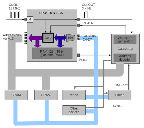
This is a simplified schematic of the addressing mechanism in the Geneve.
The CPU, the TMS 9995, contains an own set of memory locations at addresses >F000 to >F0FB and the remaining 4 bytes at the end of the address space, that is, >FFFC to >FFFF (which are the NMI (None Maskable Interrupt) branch vector). The internal memory locations are directly connected to the 16 bit data bus, so we should say these are 128 words of 16 bit each.
All other memory locations are outside of the CPU, and the 16 bit data transfers are converted to a sequence of two 8 bit data transfers. This is quite similar to the mechanism used in the TI-99/4A, with the exception that the TI send the odd address byte first, then the even address, and the TMS 9995 starts with the even address, followed by the odd address.
Wait states can only be created outside of the CPU; there is no way of creating wait states within the CPU (possibly also no need). There is a special PIN called READY which is used for wait state creation.
Instead, we have an external wait state generation. The gate array circuit is used to create wait states in certain situations. When a wait state shall appear, the READY line of the CPU must be pulled down (cleared).
One wait state has the exact duration of one cycle which is 333.3 nanoseconds. Three millions of them last for one second.
Apart from the permanent wait state, the CPU itself does not create any wait state. This should be considered when only internal accesses are done: If code is running within the internal CPU RAM, wait states have no effect. They have only effect for external memory accesses.
Timing diagrams
Some diagrams may help to understand the concept of wait states on the Geneve. I picked some of the lines, but there are some more, also important ones. If you are interested in the exact set of signal lines please see the TMS9995 specification. For now, we only discuss wait state generation.
Cycles are defined as starting from halfway of the low level, containing the whole high level, and ending at half of the time of the next down level. If we use one letter as one quarter of a cycle, it would read as LHHL. In the diagrams, each cycle has an own backdrop which differs from the next.
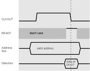
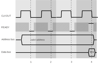
This is the timing diagram for reading from external memory. A read operation starts with the address lines (A0-A15) being set to some value. For example, when the CPU wants to read from >1000, A3 is set to 1 while the remaining address lines are set to 0.
Next we expect that the device (like RAM, video, etc.) puts the value of the given address on the data bus. Depending on the device, the requested data may be available after some delay time, or the lines may be unstable until that time has passed. The CPU waits for the falling edge of the CLKOUT signal. At that point it first checks the READY line, and if it is high as shown here, the data lines are sampled, and the memory read access is complete. After that the program counter is increased and the next access may start.
Notice that the READY line may have any value (0 or 1) at other times; we symbolize this with the hashed stripe.
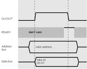
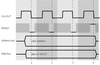
For writing the diagram looks a bit different, but still familiar. Again we omit some lines like WE line (write enable) for now. Different to reading, the writing process requires that the data bus be set shortly after the address is set. This is clear, since we must assume that the addressed device immediately fetches the values once the address is set. The CPU has no influence on the behavior of the device.
The external device may require some more time before the processing can continue; in this case it may lower the READY line; the CPU will test the line on the next falling CLKOUT edge. When it is high, as shown here, the memory write is complete, and the CPU continues with the next cycle, advancing the program counter. Remember that the CPU ignores the READY line when the memory access was directed to the internal memory locations, so in that case, the memory access is always complete at the end of the cycle.
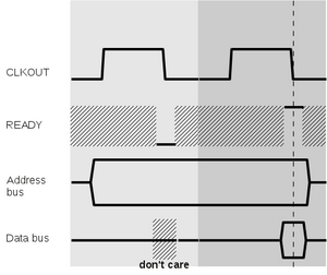
Now we have a look at the situation when a wait state is inserted. Here, a read operation is delayed by one cycle; this is typically the case when the Geneve uses its DRAM.
The memory read access starts as above, but at the first CLKOUT falling edge, the READY line is low. Now if this read access is actually an external access (and not to the on-chip RAM), the CPU skips the sampling of the data bus and waits for another falling CLKOUT edge. At that point we are at the same situation as above, and the access is complete.
What happens if we have multiple wait states? On the left side we can see a read access; as expected, the CPU loops until the READY line is high, and at that point it reads the values from the data bus. When writing, the CPU again attempts to assign the values shortly after the rising edge of CLKOUT, which is also used by the external device as the moment after which data may be safely read. The external device pulls down the READY line for this and another two cycles. This causes the CPU to loop until it finds a high READY level.
From this we learn two important points for creating wait states:
- When reading, wait states should occur before the actual read operation. Once the READY line is high, the memory access is considered as complete by the CPU, and it will advance its program counter and continue with the current or the next command. If the READY line is lowered afterwards it will only affect the following processing.
- When writing, wait states must start with the first cycle and continue for the desired times, with the last cycle showing a high READY line. Once the READY line is high, the operation is complete.
Byte accesses and word accesses
The TMS9995 is a 16 bit CPU, and as such all commands occupy two, four, or six bytes (including the arguments). Two bytes are also called a word (for 16 bit machines).
The on-chip RAM is word-addressable. That is, all words and each operand can be read in one memory cycle. If only one byte needs to be read or written, the RAM can also be addressed by byte locations (which is an important difference to the TMS9900 operation and considerably increases the efficiency of the TMS9995).
However, when we use external memory, all commands and arguments must be read by two cycles each, since the data bus only has 8 lines outside of the CPU. This has a visible impact on performance, especially when wait states are used.
Example:
F000: MOV R1,@>F080
If the workspace is located in the on-chip RAM (e.g. at >F040) we get 4 cycles for this operation:
- read the instruction MOV R1,@... : 1 cycle
- read the contents of R1 (>F042, >F043): 1 cycle
- read the target argument (F080): 1 cycle
- write the contents to the target address: 1 cycle
which makes 4 cycles or 1.332 µs execution time.
For a better overview we can use the following style:
| 1 | 2 | 3 | 4 |
|---|---|---|---|
| MOV R1,@ | < R1 | F080 | > *F080 |
If the workspace is located in DRAM instead, we get more cycles:
- read the instruction MOV R1,@... : 1 cycle
- read the contents of >F042: 1 wait state, 1 read cycle = 2 cycles
- read the contents of >F043: 1 wait state, 1 read cycle = 2 cycles
- read the target argument (F080): 1 cycle
- write the contents to the target address: 1 cycle
| 1 | 2 | 3 | 4 | 5 | 6 | 7 |
|---|---|---|---|---|---|---|
| MOV R1,@ | wait | < R1 HB | wait | < R1 LB | F080 | > *F080 |
together 7 cycles or 2.331 µs.
Now for the slowest option, assuming that we have a DRAM at the location 3000:
3000: MOV @>3800,@>3802
| 1 | 2 | 3 | 4 | 5 | 6 | 7 | 8 | 9 | 10 |
|---|---|---|---|---|---|---|---|---|---|
| wait | MOV R1,@ (HB) | wait | MOV R1,@ (LB) | wait | 38 | wait | 00 | wait | < *3800 |
| 11 | 12 | 13 | 14 | 15 | 16 | 17 | 18 | 19 | 20 |
|---|---|---|---|---|---|---|---|---|---|
| wait | < *3801 | wait | 38 | wait | 02 | > *3802 | wait | > *3803 | wait |
together 20 cycles (6.66 µs).
Wait states per device type
On-chip RAM
This one cannot have any wait state, as we stated above, since the access occurs within the CPU, and the READY pin is ignored. Reading and writing is the same case.
SRAM access
SRAM accesses by default do not create wait states. That means that the only slowdown compared to the chip-internal memory comes from the fact that we need two accesses to external memory where one access would have sufficed internally. This may indeed become expensive:
INC R1
requires 3 cycles when the code and the workspace is in the on-chip RAM (get the instruction, read the contents of R1 and increase them, write the contents of R1). As you see, the TMS9995 is able to do pipelining, which can be seen here. The instruction actually only requires three cycles although we have four activities. This is another reason why the Geneve is so much faster than the TI, although both use the same clock speed.
If the workspace were in SRAM, we would need 5 cycles (two cycles each for reading and writing to R1). If the command were in SRAM also, we get 6 cycles.
When the CRU bit at address 1EFE is set to 0, the Gate array produces extra wait states. In the case of SRAM accesses, two wait states are inserted before the read access. For write accesses, two wait states are included, starting with the access. This means that the above command when running in SRAM and with workspace in SRAM requires 18 cycles instead of 6.
DRAM access
For each DRAM access, the gate array creates by default 1 wait state. That means that for word accesses (like CLR or MOV), two wait states will be created. Again with the example
INC R1
running in DRAM with R1 in DRAM as well, we get 6 memory accesses with 2 cycles each, that is, 12 cycles.
With extra wait states, the Gate array adds another wait state for reading and writing. This means that SRAM and DRAM accesses operate at exactly the same speed.
Devices
For external bus accesses (to the peripheral box), wait states are used just as if accessing DRAM. That is, in the normal case, one WS is inserted for reading and writing. With extra wait states, two WS are inserted.
These wait states apply to
- the video processor (apart from the "background" wait states; see below)
- the memory map registers
- the keyboard interface
- the clock chip
- the sound chip (also see below)
- the GROM simulator in the Gate Array
- the cards in the Peripheral Expansion Box.
Video operation
As known from the TI-99/4A, accesses to the Video Display Processor must be properly timed, since the VDP does not catch up with the higher speed of the CPU. In fact, using a dedicated video processor turns the TI and Geneve into a multiprocessor machine, in contrast to other home computers of that time.
As we have independent processors, a synchronization line is usually required to avoid access operations at times when the other processor is not ready. However, there is no such line in the TI and Geneve. Texas Instruments recommends to insert commands to take some time before the next access, like NOPs or SWPB.
When bytes are written in a too fast succession, some of them may be lost; when reading, the value may not reflect the current video RAM contents. Setting the address may also fail when writing too quickly. The V9938 video processor of the Geneve offers its command completion status in a registered that can be queried from a program, but there is no synchronization by signal lines.
The problem has become worse with the higher performance of the Geneve. This may mean that programs that worked well with the TI may fail to run on the Geneve because of VDP overruns. For this reason, wait states may be inserted for video operations.
The Geneve generates two "kinds" of wait states when accessing the VDP. The first kind has been explained above; the VDP is an external device and therefore gets one wait state per default, and two when extra wait states are selected. After the access, however, the Gate Array pulls down the READY line for another 14 cycles when the CRU bit for video wait states is set (address 0x0032 or bit 25 when the base address is 0x0000).
There are some interesting points about video wait states, which we discuss in a separate section.
Sound chip
Wait state generation for the sound access seems to be confusing at first. Unlike all previous experiments, the ones with sound access did not yield exact delay times. For instance, with different numbers of intermediate lines, the line with the sound access seems to change its number of wait states. Measurements show that we have discrete execution times (e.g. 32, 40, or 53 cycles) although we add instructions that use 3 cycles, so we should be able to get 35 cycles, for instance, yet we don't.
The reason may be easier than expected: The sound chip has an own clock, and it offers a SNDRDY line which is connected to the Gate array. The number of wait states that are inserted obviously depends on the current state of the SNDRDY line. In that sense, execution is synchronized to the sound clock.
Within the MESS emulator we decided to go for an average number of 24 wait states for the sake of simplicity. When the mechanisms behind these wait states are clarified this may be realized in MESS in a similar way.
GROM simulator
The Geneve features a GROM simulator within the TI mode. GROMs are considered to be "slow" devices, driven by a clock at 400-500 MHz; in the TI-99/4A console the clock signal is delivered by the VDP (video processor).
Somewhat surprisingly, the GROM simulator in the Geneve does not apply special wait states for GROM access. One or two wait states are inserted, according to the extra wait state settings, as seen with DRAM. This is clear, since DRAM pages are used to store the GROM contents. The lack of specific GROM wait states implies that GROM access should be much faster on the Geneve than on the TI.
Automatic wait state generation
Within the Geneve, wait states can be generated to slow down operation for keeping timing constraints. The TMS 9995 CPU can create wait states itself on every external memory access by a certain hardware initialization (READY high with RESET going from low to high). This is not used in the Geneve as those wait states cannot be turned off.
