Programmable Systems Interface TMS 9901
The Programmable System Interface (PSI) is a circuit that is used on the TI-99/4A main board, on some expansion cards, and on the Geneve.
The designation of the PSI is TMS9901, and this is the name that most users should be more familiar with.
Features
The TMS 9901 Programmable Systems Interface is a multi-purpose circuit that is used in the TI-99/4A and the Geneve computer, and also on some peripheral cards like the Corcomp Floppy Disk Controller.
The 9901 has three main usage modes:
- Input/Output ports
- Interrupt prioritizing
- Timer
The I/O ports are mainly used for scanning the keyboard and joysticks, while the timer is used for cassette data encoding and decoding. The interrupt prioritizer is only used for the video interrupt which is routed from the VDP to the CPU through the 9901.
Package
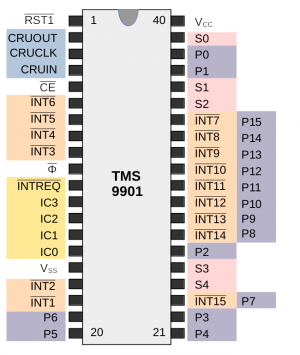
This is the pin assignment according to the 9901 specification.
You can see pins of related functions marked by the same background color.
Orange: Interrupt inputs
Red: CRU bit selection (00000 - 11111, i.e. 0-31 decimal)
Blue: CRU interface
Violet: I/O ports
Yellow: Outgoing interrupt and level
Note that some pins have a double function, or in other words, two functions share the same pin. I will discuss this in the following sections.
Input/Output port operation
The simplest way of working with the 9901 is input/output operation with the ports. The 9901 has 16 configurable ports that can be individually used as inputs or outputs: P0 to P15.
Px port as input
The power-on preset for every port is input. If you want to probe the P2 status (bit 18), use
CLR  R12
TB   18
JEQ  P2ACT
TB copies the bit at the given CRU address into the Equal bit of the status register. JEQ will jump to the location when this input has a high level. The maximum input current is 100 µA. You should protect the input with a resistor; see below for a more detailed discussion.
If you want to read all 16 ports, use the STCR instruction:
LI   R12,32
STCR R1,0
Note that the CRU base address in R12 advances in steps of 2, so bit 16 is on address 32. Also, for reading 16 bits, you must specify a count of 0.
Besides the 16 ports, the interrupt inputs of the 9901 can be used as input ports as well. More about that can be found in the section about the interrupt mode.
Px port as output
Once you write a value to the CRU address of a 9901 port, this port switches to output mode. The value written to the port is the value that is shown on its pin. If we want to output a 1 on P6, we have to use
CLR  R12
SBO  22
If we wanted to output a 0, SBZ would have to be used. In order to set several ports in one go, use LDCR.
We can also read the output port just by using TB as usual (or STCR for several ports at once).
CLR  R12
SBO  22
TB   22
JEQ  EXPECT
The TB operation should return the 1 which the previous SBO has set.
You cannot switch back to input mode. This is only possible by resetting the 9901, either using the /RST1 input line, or by setting the /RST2 bit (bit 15) to 0 in clock mode.
Interrupt mode
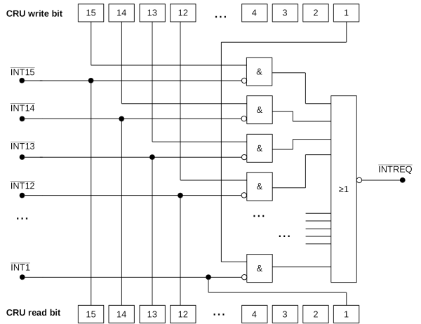
In interrupt mode, bits 1 to 15 are used to set the interrupt mask (write), or to query the interrupt inputs (read). That is, the meaning of reading and writing the bits is indeed different.
This schema shows how the interrupt inputs are used.
This illustration is slightly simplified; there is a latch between each interrupt input and the mask AND gate. This is not relevant for our programming, though. For more details see the TMS 9901 Programmable Systems Interface Data Manual [1].
Checking the interrupt inputs
In general, every interrupt input can be read via CRU access:
 CLR R12
 TB  15
 JEQ NOINT15
TB copies the bit at the specified CRU address to the Equal status bit. This means that JEQ jumps to the location when the bit is 1. Since all interrupt inputs are negative logic, reading a 1 means that there is no interrupt at this input (so I called it NOINT15).
If we want to read several interrupt inputs by a single instruction, we have to use STCR.
 LI   R12,16
 STCR R1,8
This reads the states of the /INT8, /INT9, ..., /INT15 inputs and puts them in the most significant byte of R1. (See the specification of STCR and LDCR for transfers of up to 8 bits.)
Interrupt levels
Each interrupt input (/INT1 to /INT15) may be used to trigger an interrupt at another circuit, typically the CPU. For this purpose, the 9901 offers an /INTREQ outgoing line. In the TI console, it is routed to the /INTREQ input of the TMS9900 CPU.
In addition there is a priority encoder, which is not shown here. This encoder outputs a 4-bit number which reflects the smallest number of the interrupt inputs where an interrupt has been sensed.
That is, if /INT4 and /INT7 are currently set to 0 (active), the priority encoder outputs (0100), which means 4.
The TMS9900 CPU can differentiate between these interrupt levels, and by using its LIMI command, we can set a threshold where interrupts are ignored. So when we use a LIMI 3, the interrupts of level 4, 5, 6 and higher will be ignored.
The bad news is that Texas Instruments did not use these priority lines in the TI console. In fact, these outputs (IC0 .. IC3) are not connected, and the respective interrupt level inputs at the CPU are hardwired to (0001), which means that every interrupt that occurs in the TI console is automatically set to level 1. So in order to block all interrupts from the 9901
LIMI 0
must be executed. To allow all,
LIMI 1
is sufficient. For some unclear reason, TI used LIMI 2 in all occasions.
Arming and disarming interrupts
As said above, every interrupt input can be read at any time in interrupt mode. In that sense, we don't really treat these inputs as interrupts inputs, but simply as input ports.
If we want a port to trigger an interrupt, we must arm this interrupt input. This is done by setting the respective bit to 1.
 CLR  R12
 SBO  2
This enables interrupt input /INT2 to cause an /INTREQ when its input changes to 0. In the TI console, /INT2 is connected to the interrupt output of the VDP (video processor). If you want to block interrupts on that input, use SBZ.
It is a common misunderstanding that interrupts can be cleared by using a SBZ on an input. I also found this in the popular TI Intern book. Instead, SBZ n simply blocks interrupt input /INTn. In the case of the video processor, it is up to the VDP to clear its interrupt, and this is done by reading its status register.
Consequently, you cannot read the current mask setting of the 9901. What you get from reading are the input levels of the pins. So if you plan to change the mask bits temporarily, be aware that you cannot ask the 9901 to give you the current setting which you want to restore later. You will have to find out by another way.
Clock mode
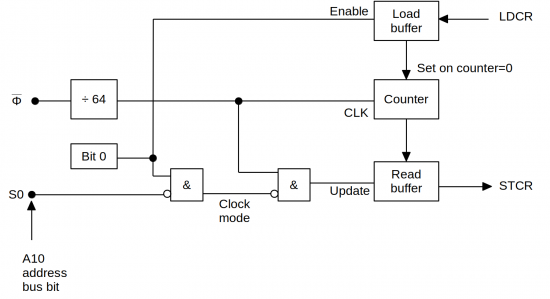
Besides the I/O capabilities, the 9901 offers a "real-time" clock. This should not be understood as a precise timer with seconds, hundreds of seconds or other but as a countdown timer that is decremented every 64 CPU clock cycles.
This schematic is taken from the Osborne book [2], redrawn by me in LibreOffice (and with added Load Buffer).
Using the timer
There are basically two ways of using the countdown timer:
- Interval timer: Set the counter to a value; wait until the counter reaches zero. The 9901 can be set up to raise an interrupt at that instant.
- Event timer: Set the counter to a value; do something and then read the counter value.
The counter has 14 bits; that is, its maximum value is 0x3FFF (16383). The counter is decremented every 64 clock cycles, and for the TI-99/4A and the Geneve with a clock cycle time of 333ns, this means that the counter resolution is 21.333 µs. The whole 16384 steps take 0.3495 seconds (349.5 ms).
When the counter reaches 0, it is reloaded from the load buffer, and counting continues.
It is essential to understand that the counter always counts down, independent of the mode. The specification says that the clock is enabled when a non-zero value is loaded into the load buffer, but tests on a real Geneve show that the clock decrements even when the load buffer is filled with 0.
Setting the timer
In order to set the load buffer and so to define the maximum counter value, we must switch to clock mode. This is done by setting bit 0 of the 9901 to 1. In the TI/Geneve systems, the 9901 is mapped to CRU base address 0, so we can do this
CLR  R12
SBO  0
to enter clock mode. Using SBZ 0 returns to interrupt mode.
The effect of switching to clock mode is that the load buffer becomes accessible by the CRU addresses 1 to 14. Supposed that we want to load the buffer with the value 0x00FF, we may use these lines:
 CLR  R12
 SBO  0
 LI   R1,>00FF
 INCT R12
 LDCR R1,14
As we see, we must change the CRU base. The LDCR operation always starts at the address defined in R12; if this is not 0, we have to set it here. Note, however, that the CRU address is always half of the R12 value, since the rightmost bit, A15, is not part of the address. If we want to start at bit 1, we must increase R12 by 2. This is, by the way, done wrong in several places in the literature where R12 is only set to 1.
We can combine the SBO and the LDCR to one operation if we define the rightmost bit of R1 as the bit 0 and the following bits as the timer value.
 CLR  R12
 LI   R1,>01FF    (0000 0001 1111 1111)
 LDCR R1,15
Do not write all 16 bits. The last bit will change bit 15 of the 9901, which is the /RST2 bit. When we are in clock mode, writing a 0 to the /RST2 bit resets all I/O ports. This means that all pins are set to inputs, and devices that rely on them as outputs may be turned off unintentionally.
Reading the timer
We are interested for the current value of the timer at some occasions. However, since the counter is constantly changing (every 64 clock cycles), reading from the active counter may deliver a wrong result. Think, for instance, about a value 0x2000, which is decremented after we read the first bits, we may end up with 0x2FFF (2 from 0x2000, FFF from 0x1FFF).
For this reason, the timer value is copied to a read buffer. This happens at every 64th clock cycle, when the counter is also decremented, but only when we are not in clock mode.
To read the buffer, we must set the 9901 to clock mode first, which freezes the counter value in the read buffer. Then we can read the counter using STCR.
 CLR  R12
 SBO  0
 STCR R1,15
 SRL  R1,1
 SBZ  0
As we see, register 1 will contain bit 0 in its rightmost bit, so we shift R1 by one position to move it out.
Do not forget to return to interrupt mode, or the buffer will not receive further updates.
As mentioned, bit 15 is the /RST2 bit when we write to it. For reading, bit 15 reflects the /INTREQ output.
The weird S0 input
There is one peculiarity with the 9901. When the input line S0 is set to 1, the clock mode is left temporarily - until S0 is 0 again, and bit 0 is 1. If bit 0 is 0, this has no effect, as the clock mode is never entered.
What is the reason for this?
TI obviously considered use cases where the 9901 remains in clock mode for longer times, while the I/O ports must still be operated. The I/O ports are available on bits 16-31, which means that the S0 input is 1 for these addresses. So when we do a SBO 16, this is not related to the timer value, and thus should control the first I/O port. To allow this, the chip returns to interrupt/port mode for this operation, and when S0 is reset, returns to clock mode.
In the TI console, the S0-S4 inputs are directly connected with the address bus lines A10-A14. This has a strange side effect: Whenever address bus line A10 changes to 1, the clock mode is left temporarily, and this also happens for ordinary memory accesses.
Suppose that we are in clock mode (SBO 0). In this mode, the read buffer should not be updated, so when we read it, we should get the same value every time, although the real counter value is different. But this is difficult to achieve: If our program uses a memory address where A10 is 1 for some instruction, loading this instruction into the CPU will set A10 to 1, and thus leave clock mode, which updates the counter.
Therefore, you may have the impression that the read register continues to be updated even though you set bit 0 to 1. But this is only happening because your program extends over a location where A10 is 1. So if you want to prove that in clock mode the read register remains fixed, your program must avoid all memory locations where A10 is 1.
Some pins have a double meaning; for example, pin 34 is labeled /INT7 / P15. How do we select the functions?
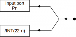
The shared pins are those for the interrupt inputs /INT7 to /INT15; they may also be used for P7 to P15 (in the opposite order).
If the Pn port is set to input, the situation looks like this:
This means that both port and interrupt input have the same values; each one is a mirror of the other's state. We notice it by reading the bits of the associated CRU addresses, getting the same results. There is a difference, though: The interrupt input can be armed to trigger an outgoing interrupt, while the I/O port cannot.
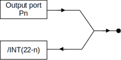
In the other case, the Pn port is an output.
Is that possible? - Sure. The interrupt input will reflect the output of the port. When we set the port to 1, the interrupt input will get that 1 (same for 0). If we arm the interrupt input, setting the output port to 0 will trigger an interrupt via this input. The 9901 specification document recommends to disarm the interrupt trigger for the shared ports because of this possibly unwanted effect.
Safety precautions
The TMS9901 PSI is an interrupt encoder and an I/O circuit. You may have heard that improper use of I/O circuits may damage the circuit so that it must be replaced. Is this possible with the 9901 as well? Is there a way to kill the 9901?
Short answer: Yes.
Longer answer: Yes, but it depends on the way how the ports are used.
If the port is used as an input, nothing bad will happen, since the ports have high input impedance. You can put 0V or 5V directly to the input; of course, you should not use excessive voltage.
How to damage the 9901 ports
The problem is when the port is configured as an output port. In that case it may output 0V (0) or 5V (1). When you connect the output to the opposite voltage, you will cause a short circuit which quickly exceeds the chip's maximum power dissipation of 750 mW. This means you will fry the chip.
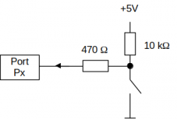
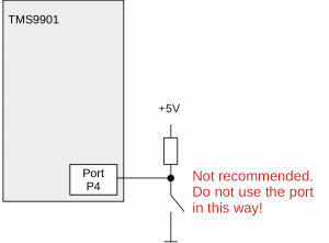
Consider the following setup (but don't try it!).
Obviously, port P4 is assumed to be an input. When the switch is open, port P4 will sense a 1 on its input. When the switch is closed, it will sense a 0.
Now what happens when you execute this code?
CLR  R12
SBO  20
This will program port P4 to be an output, and to show a 1 (5V) at the output. SBZ will, in contrast, make this port output a 0. So how do you make it an input port? - This is done by resetting the chip. As long as you don't use a SBZ/SBO (or a LDCR) on the ports, the ports are inputs.
Nothing has happened up to now. But now imagine that you press the switch. This will put the 1 output to ground, causing the short circuit, and your 9901 is toast.
What about the TI console?
So can we damage the 9901 in the TI console by a suitable CRU operation? - Luckily not.
The reason is the way TI used the ports on the mainboard. Most of the ports are configured as outputs. Nothing happens when you reset them to inputs.
- The pure interrupt inputs (/INT1 to /INT6) are safe, as they cannot output anything. They have no output driver that could be fried.
- P0 and P1 are not connected.
- P2, P3, and P4 are designed as outputs, so they cannot be turned from an input to an output.
- P5 is the selector of the Alpha Lock key, so output as well.
- P6 and P7 (/INT15) are the cassette motor control outputs.
- P8 (/INT14) is the audio gate output.
- P9 (/INT13) is the cassette output.
- P10 (/INT12) is pulled up to 5V via a 10 kOhm resistor. If you put a 0 on this port (5V), the maximum current is 500 µA, which results in a power dissipation of 2.5 mW (far below the maximum 750 mW).
- P11 (/INT11) is the cassette input. However, there is a resistor of 2.2 kOhm (R413) which effectively guards the port of high currents.
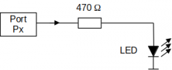
- P12, P13, P14, P15 (/INT10 ... /INT7) are the keyboard input lines. Again, we have pull-ups of 10 kOhm against +5V, but also 470 Ohm on the line, which means a maximum of 8.5 mA or 42.5 mW. This is still well below the maximum value.
So we see that resistors are the best way to protect the ports. And we may calm down; we cannot burn the 9901 in the TI console by a bug in our program.
Literature
[1] Texas Instruments: TMS 9901 Programmable Systems Interface Data Manual, July 1977
[2] Adam Osborne, Gerry Kane: Osborne 16-Bit Microprocessor Handbook / Includes 2900 Chip Slice Family. Published by OSBORNE/McGraw-Hill 1975, 1981. ISBN 0-931988-43-8.
